
 This is a small adapter board to allow Atmel’s ATtiny24/44/84 µController chip to be used on the Atmel STK500 development platform.
Description
I recently wanted to use one of Atmel’s smaller chips on a project and selected the ATtiny84 – it’s one of a family of chips with varying memory amounts. The Attiny24 has 2K bytes of flash ram, the 44 has 4K, and the 84 has 8K. It comes in a DIL package but I’m more interested in the SOIC surface mount version. The problem is, the Atmel STK500 development platform I’m using does not support either chip natively.
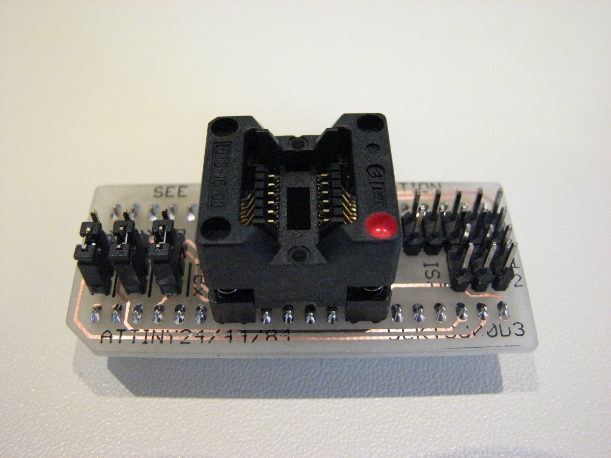
Atmel does offer an adapter board to support this chip along with another one with slightly more I/O lines. The STK505 adapter, which is reasonably priced at US$75, would be a great solution. Unfortunately, I’m stuck in China and it’s not available over here. So… it’s time for a roll-your-own solution. While a lot of things are not available over here, SOIC ZIF test sockets are, and are priced very inexpensively at only US$8. I originally thought I’d get one DIL version of the chip for development work on the STK500, but realized I’d rather use the SMD version on any project I did (since I’m making my own boards, it’s easier to work with SMD components because I don’t have to do any drilling). So, with cheap SOIC sockets available, and no STK505 available, this is what I came up with:
 Like the STK505 adapter, my little adapter allows ISP and HV programming. It has jumpers (instead of switches as on the ‘505) to control the dual nature of some of the PORTB pins on the Tiny24 – PB1, PB2, and PB3 are used as the RESET, XTAL1, and XTAL2 connections for this reduced pin-count chip. They can also be used as normal I/O pins if these functions are not needed.
The STK505 has switches to control these functions. My little adapter board uses standard 0.025″ square pin headers and jumpers because of the limited board real estate. Besides the three jumper blocks on the front of the board, there is a 6-pin ISP programming header and a 10 pin High Voltage programming header behind the ZIP socket. These function identically to the corresponding headers on the STK505.
One additional change from the STK505, is the use of the STK500’s on-board crystal/SW oscillator instead of the adapter mounted crystal on the ‘505.
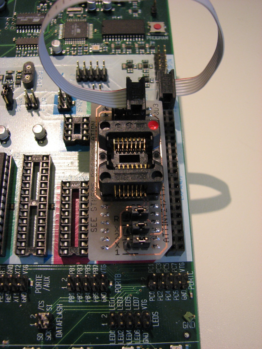
The usage instructions in the STK505 User Guide also cover this adapter board. The adapter board fits in the SCKT3000D3 40-pin socket on the STK500 as shown in the photo.
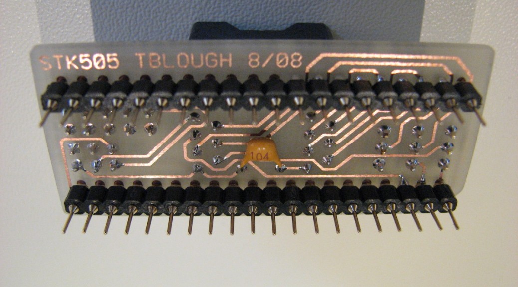
 The double-sided board was made in the kitchen sink using the “toner-transfer” method. Since this was a home-made board without plated through holes, the components themselves were used to provide signal paths from one side of the board to the other and therefore must be soldered on both sides.
Consideration also had to be given to components (like the ZIF socket) that could not be soldered on both sides. When routing the board, these components had to have all connections made on one side of the board only. I’m happy to say that by using the component leads to shuttle signals from one side of the board to the other, the board was laid out without any vias. This makes it a little easier to build, but means that you really need to think about the construction order before commencing. The build notes describe the process I followed.
Disclaimer and License
It worked for me so it should work for you, but no guarantees. Feel free to use the schematics and information on this page as you see fit, but a little attribution would be appreciated.
Project Sources
- Cadsoft Eagle Files (23K .zip)
- Build notes (2K .txt)
- Atmel STK505 User Guide (Atmel)
Build Notes
I named this an STK505 clone, but it's really just an adapter board that plugs into
an STK500 to use the ATtiny24/44/84 devices in the 14-SOIC package.  See the
STK505 user guide for instructions on how to use the adapter for High Voltage
Serial Programming.

Build hints

1) This board is made using the toner transfer procedure and therefore does not
have plated through holes.  Because of this many components need to be soldered
on both sides of the board.

2) Begin by installing the XTAL2 header.  Solder all three pins on the bottom of the
board.  Gently lift the black plastic spacer up to the top of the pins and sparingly
solder pin 1 on the top (the one with the trace connected).

3) Following the above procedure mount the XTAL1 and RESET headers soldering the
respective connections on the top that have traces connected.

4) Using the same procedure as in #2, mount the ISP header, then finally the HV
programming header

5) Mount the bypass cap on the bottom of the board and solder both top and bottom
sides.  Clip the leads on the top very close to the board because the SOIC socket
needs to fit over these pads.

6) Use turned pin IC socket headers, like in the photo of the bottom of the board.
This facilitates soldering on both sides of the board.  Before loading onto the board,
clip pins 7, 8, 13, 14, 27, and 28 off the top side of the headers.  This will allow
the SOIC socket to fit flush.

7) Place the headers in the board and load the board into a 40 pin IC socket to
help align the pins (the socket on the STK500 works fine if you solder quickly).
Solder the headers to the top side of the board.

8) Solder the pins on the bottom of the board where there are trace connections
(pins 1, 2, 3, 9, 32, 34, 35, 36, 37, 38, and 39).

10) Clip pins 33 and 34 very close on the top of the board so the SOIC socket can
seat correctly.

11) The socket I used, an Enplas OTC-16-03, needs a little modification before mounting.
I could not find a 14 pin socket so I disassembled the 16 pin socket and removed the
contact fingers for pins 8 and 9 in a 16 pin socket.  Reassemble the socket and
cut the two locating pins off the bottom.  File the remaining protrusions flush with
the bottom of the socket and file the standoff boss that will end up over pins
33 and 34 off flush as well.

12) Finally solder the socket, clean the board and push the plastic pin header
strips back down to the board.